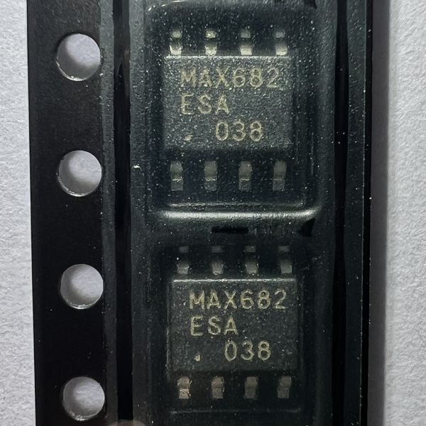
The MAX682ESA, produced by Maxim Integrated, is a regulated 5V-output charge pump integrated circuit. Charge pumps are electronic circuits that generate a higher voltage from a lower voltage power source through a process of stepping up the voltage.
Here are some details about the MAX682ESA:
- Part Number: MAX682ESA
- Type: Regulated 5V-Output Charge Pump
- Package/Case: 8-SOIC (Small Outline Integrated Circuit)
- Input Voltage: Typically operates from 1.5V to 5.5V
- Output Voltage: 5V (regulated)
- Switching Frequency: Typically operates at several hundred kilohertz
- Efficiency: Provides high efficiency voltage conversion
- Features: Low Quiescent Current, Short-Circuit Protection, Thermal Shutdown Protection
Purpose:
The purpose of the MAX682ESA is to provide a regulated 5V output from a lower voltage power source, offering a convenient way to power circuits that require a 5V supply from a lower voltage source.
Application:
This IC can be utilized in a variety of applications, including but not limited to:
- Battery-Powered Devices: Used in portable electronics where a stable 5V supply is needed from a lower voltage battery source.
- Compact Electronics: Ideal for space-constrained applications where a separate 5V power supply might not be feasible.
Benefits:
- Efficiency: Provides efficient voltage conversion, ensuring optimal power usage.
- Regulated Output: Offers a stable and reliable 5V output, crucial for sensitive digital circuits and analog components.
- Protection Features: Incorporates protections such as short-circuit and thermal shutdown to ensure robust and safe operation.
In summary, the MAX682ESA by Maxim Integrated is a regulated 5V-output charge pump IC designed to provide a stable 5V output from a lower voltage power source. This makes it suitable for various low-power and portable electronics applications, ensuring reliable and efficient power delivery in space-constrained environments.
| DataSheet | MAX682ESA PDF |
|---|


